| CPC H01L 21/823814 (2013.01) [H01L 21/28518 (2013.01); H01L 27/0924 (2013.01)] | 20 Claims |
|
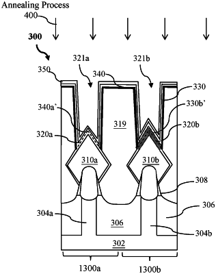
1. A semiconductor structure, comprising:
an N-type transistor that includes:
a first fin structure comprising a source/drain region;
a first transition source/drain feature disposed over the source/drain region of the first fin structure;
a first source/drain feature disposed on the first transition source/drain feature; and
a metal germanide layer disposed on the first source/drain feature,
wherein the first transition source/drain feature and the first source/drain feature comprises silicon and an n-type dopant,
wherein a concentration of the n-type dopant in the first transition source/drain feature is smaller than a concentration of the n-type dopant in the first source/drain feature.
|