| CPC H01L 21/823481 (2013.01) [H01L 21/02148 (2013.01); H01L 21/02159 (2013.01); H01L 21/02164 (2013.01); H01L 21/0217 (2013.01); H01L 21/02178 (2013.01); H01L 21/02181 (2013.01); H01L 21/02183 (2013.01); H01L 21/02186 (2013.01); H01L 21/02189 (2013.01); H01L 21/0228 (2013.01); H01L 21/76224 (2013.01); H01L 21/823431 (2013.01); H01L 27/0886 (2013.01); H01L 29/0653 (2013.01)] | 20 Claims |
|
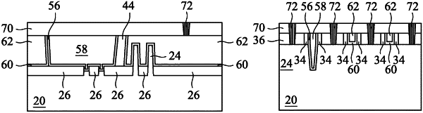
1. A structure comprising:
a first fin on a substrate;
a second fin on the substrate, the first fin and the second fin being longitudinally aligned;
a third fin on the substrate;
a first insulating region and a second insulating region, the first fin and the second fin being between the first insulating region and the second insulating region, wherein the first fin and the second fin extend above an upper surface of the first insulating region and the second insulating region; and
a gate structure extending over the third fin;
a first gate spacer on a first side of the gate structure;
a second gate spacer on a second side of the gate structure;
a fin cut-fill structure disposed between the first fin and the second fin, the fin cut-fill structure comprising:
an insulating liner along sidewalls of the first gate spacer and the second gate spacer, the insulating liner comprising a material with a band gap greater than 5 eV; and
a fill material, the insulating liner surrounding the fill material in a plan view.
|