| CPC H01L 21/823468 (2013.01) [H01L 21/823431 (2013.01); H01L 27/0886 (2013.01); H01L 29/0665 (2013.01); H01L 29/42392 (2013.01); H01L 29/6653 (2013.01); H01L 29/66545 (2013.01); H01L 29/66553 (2013.01); H01L 29/6656 (2013.01); H01L 29/66795 (2013.01); H01L 29/78696 (2013.01)] | 20 Claims |

|
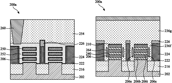
17. A method for forming a semiconductor device, comprising:
forming a fin structure including two or more channel layers and two or more spacing layers formed between the two or more channel layers;
forming cladding layers on sidewalls of the fin structure;
forming hybrid fins adjacent the cladding layers;
depositing a sacrificial gate electrode layer over the fin structure, the cladding layers and the hybrid fins;
patterning the sacrificial gate electrode layer to form a sacrificial gate structure;
forming trenches between the sidewalls of the fin structure and the hybrid fins by removing the cladding layer exposed by the sacrificial gate structure;
depositing an insulating material on the sacrificial gate structure and in the trenches between the sidewalls of the fin structure and the hybrid fins, wherein air gaps are formed in the trenches between the sidewalls of the fin structure and the hybrid fins;
recess etching the fin structure;
recess etching the two or more spacing layers to form inner spacer cavities;
forming inner spacers in place of the recessed spacing layers; and
forming source/drain features.
|