| CPC H01L 21/78 (2013.01) [H01L 21/268 (2013.01); H01L 21/4853 (2013.01); H01L 21/563 (2013.01); H01L 22/32 (2013.01); H01L 23/3185 (2013.01); H01L 23/544 (2013.01); H01L 24/16 (2013.01); H01L 2223/5446 (2013.01); H01L 2224/16225 (2013.01); H01L 2924/18161 (2013.01); H01L 2924/35121 (2013.01)] | 19 Claims |

|
1. A method for producing a semiconductor device, the method comprising:
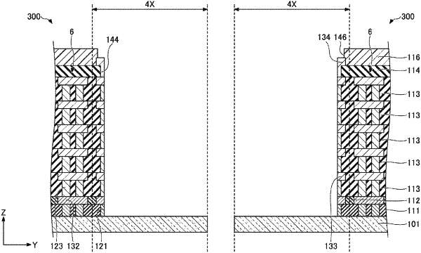
removing a first pad located in a first area of a first scribe area of a semiconductor wafer by emitting laser beam along a first direction, the first scribe area extending in the first direction in a plan view, the first area extending in the first direction in a plan view; and
dicing a second area of the first scribe area of the semiconductor wafer after removing the first pad, the wafer including a circuit area, the second area extending in the first direction in a plan view, and the first area being located between the second area and the circuit area in a second direction which is different from the first direction in a plan view,
wherein the first area of the first scribe area is separated from the second area of the first scribe area in a plan view.
|