| CPC H01L 21/78 (2013.01) [H01L 21/71 (2013.01); H10B 43/27 (2023.02)] | 21 Claims |
|
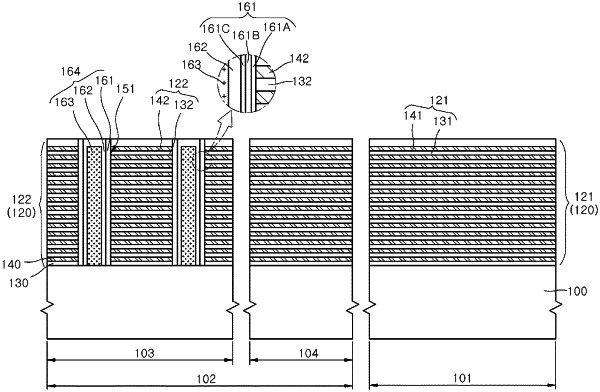
1. A method of manufacturing a semiconductor chip, the method comprising;
forming a layer stack in which first material layers and second material layers are alternately stacked over a semiconductor substrate that includes a chip region and a scribe lane region; and
forming crack propagation guides in a first portion of the layer stack within the scribe lane region.
|
|
16. A method of manufacturing a semiconductor chip, the method comprising:
forming a first layer stack in which first material layers and second material layers are alternately stacked over a semiconductor substrate that includes a chip region and a scribe lane region;
forming a first channel hole that substantially vertically penetrates a second portion of the first layer stack that overlaps with the chip region;
forming a sacrificial layer that fills the first channel hole;
forming a second layer stack in which third material layers and fourth material layers are alternately stacked on the first layer stack and the sacrificial layer;
forming a second channel hole that substantially vertically penetrates a second portion of the second layer stack that overlaps with the chip region and is connected to the first channel hole together with openings that substantially vertically penetrate a first portion of the second layer stack within the scribe lane region;
removing the sacrificial layer through the second channel hole;
forming memory layers, channel layers, and fillers on sidewalls of the first and second channel holes;
forming crack propagation guides that fill the openings;
irradiating portions of the semiconductor substrate that overlaps with the crack propagation guides with a laser to generate cracks in the portions of the semiconductor substrate; and
separating semiconductor chips from the semiconductor substrate by propagating the cracks while a crack propagation direction is guided by the crack propagation guides.
|
|
21. A method of manufacturing a semiconductor chip, the method comprising:
forming a layer stack in which a first material layer and a second material layer are alternately stacked over a semiconductor substrate that includes a chip region and a scribe lane region;
forming a first channel hole that substantially vertically penetrates a second portion of the first layer stack that overlaps with the chip region together with openings that substantially vertically penetrate a first portion of the first layer stack within the scribe lane region;
forming sacrificial layers that fill the first channel hole and the openings to form crack propagation guides with portions of the sacrificial layer that fill the openings;
forming a second layer stack in which a third material layer and a fourth material layer are alternately stacked on the first layer stack and the sacrificial layers;
forming a second channel hole that substantially vertically penetrates a second portion of the second layer stack that overlaps with the chip region and is connected to the first channel hole;
removing another portion that fills the first channel hole of the sacrificial layer through the second channel hole;
forming memory layers, channel layers, and fillers on sidewalls of the first and second channel holes;
irradiating portions of the semiconductor substrate that overlaps with the crack propagation guides with a laser to generate cracks in the portions of the semiconductor substrate; and
separating semiconductor chips from the semiconductor substrate by propagating the cracks while a crack propagation direction is guided by the crack propagation guides.
|