| CPC H01L 21/78 (2013.01) [H01L 21/30655 (2013.01); H01L 21/0275 (2013.01); H01L 21/3081 (2013.01); H01L 21/31127 (2013.01); H01L 22/34 (2013.01)] | 4 Claims |
|
1. A device chip manufacturing method for dividing a silicon wafer formed with devices in each of regions of a front surface partitioned by a plurality of mutually intersecting streets, into individual device chips, the device chip manufacturing method comprising:
a resist film coating step of coating the front surface of the silicon wafer with a resist film;
an exposing step of removing the resist film in regions along the streets to expose the silicon wafer;
a silicon wafer conveying-in step of conveying the silicon wafer into a plasma etching apparatus;
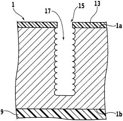
a deep groove forming step of alternating a plurality of times between isotropic etching using a plasma of a CF4 gas or an SF6 gas and coating of regions exposed by the isotropic etching with a passivation film by use of a plasma of a C4F8 gas to process the silicon wafer along the streets, thereby forming deep grooves not reaching a back surface of the silicon wafer; and
a dividing step of subjecting bottom portions of the deep grooves to anisotropic etching by use of a plasma of a mixed gas of SF6 and O2 to form division grooves reaching the back surface of the silicon wafer, thereby dividing the silicon wafer into the individual device chips.
|