US 11,990,370 B2
Methods for forming conductive vias, and associated devices and systems
Trupti D. Gawai, Boise, ID (US); David S. Pratt, Meridian, ID (US); Ahmed M. Elsied, Boise, ID (US); David A. Kewley, Boise, ID (US); Dale W. Collins, Boise, ID (US); Raju Ahmed, Boise, ID (US); Chelsea M. Jordan, Boise, ID (US); and Radhakrishna Kotti, Meridian, ID (US)
Assigned to Micron Technology, Inc., Boise, ID (US)
Filed by Micron Technology, Inc., Boise, ID (US)
Filed on Oct. 21, 2022, as Appl. No. 18/048,633.
Application 18/048,633 is a continuation of application No. 17/136,287, filed on Dec. 29, 2020, granted, now 11,515,204.
Prior Publication US 2023/0113573 A1, Apr. 13, 2023
This patent is subject to a terminal disclaimer.
Int. Cl. H01L 21/768 (2006.01); H01L 23/522 (2006.01); H01L 23/528 (2006.01)
CPC H01L 21/76883 (2013.01) [H01L 21/76816 (2013.01); H01L 23/5226 (2013.01); H01L 23/5283 (2013.01)] 20 Claims
OG exemplary drawing
 
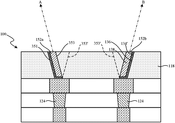
1. A semiconductor device, comprising:
a first layer of insulative material;
a second layer of insulative material over the first layer;
an electrically conductive feature extending through the first layer; and
an electrically conductive via extending through the second layer and electrically coupled to the electrically conductive feature, wherein the electrically conductive via includes a pair of generally parallel first sidewalls, and wherein the electrically conductive via extends along an axis that is slanted relative to the first layer of insulative material.