| CPC H01L 21/76877 (2013.01) [H01L 21/02118 (2013.01); H01L 21/31133 (2013.01); H01L 21/76834 (2013.01); H01L 21/76837 (2013.01); B05D 1/60 (2013.01); B05D 1/62 (2013.01)] | 20 Claims |
|
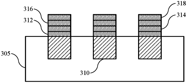
1. A semiconductor processing method comprising:
forming a layer of carbon-containing material on a substrate disposed within a processing region of a semiconductor processing chamber, wherein the substrate comprises an exposed region of a first dielectric material and an exposed region of a metal-containing material, wherein the layer of carbon-containing material is selectively formed over the exposed region of the metal-containing material, and wherein forming the layer of carbon-containing material comprises one or more cycles of:
providing a first molecular species that selectively couples with the metal-containing material, and
providing a second molecular species that selectively couples with the first molecular species; and
selectively depositing a second dielectric material on the exposed region of the first dielectric material.
|