US 11,990,367 B2
Apparatus and memory device including conductive lines and contacts, and methods of forming an apparatus including conductive lines and contacts
Xiaosong Zhang, Boise, ID (US); Yongjun J. Hu, Boise, ID (US); David A. Kewley, Boise, ID (US); Md Zahid Hossain, Boise, ID (US); Michael J. Irwin, Boise, ID (US); Daniel Billingsley, Meridian, ID (US); Suresh Ramarajan, Boise, ID (US); Robert J. Hanson, Boise, ID (US); Biow Hiem Ong, Singapore (SG); and Keen Wah Chow, Singapore (SG)
Filed by Micron Technology, Inc., Boise, ID (US)
Filed on Aug. 12, 2021, as Appl. No. 17/444,948.
Application 17/444,948 is a continuation of application No. 16/542,507, filed on Aug. 16, 2019, granted, now 11,101,171.
Prior Publication US 2021/0375670 A1, Dec. 2, 2021
Int. Cl. H01L 21/768 (2006.01)
CPC H01L 21/76831 (2013.01) [H01L 21/76843 (2013.01); H01L 21/76879 (2013.01); H01L 21/76804 (2013.01)] 20 Claims
OG exemplary drawing
 
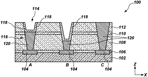
1. An apparatus comprising:
conductive elements underlying an insulative material;
conductive lines operably coupled to the conductive elements; and
contacts intersecting the conductive lines and extending from upper surfaces of the conductive lines to upper surfaces of the conductive elements with the contacts directly adjacent to the insulative material and the conductive elements, an outer diameter of the contacts at an elevation of the upper surfaces of the conductive lines is greater than a width of the conductive lines external to the contacts.