US 11,990,366 B2
Semiconductor device and method for manufacturing the same, and electronic apparatus
Suguru Saito, Kanagawa (JP); Nobutoshi Fujii, Kanagawa (JP); Masaki Haneda, Kanagawa (JP); and Kazunori Nagahata, Kanagawa (JP)
Assigned to SONY SEMICONDUCTOR SOLUTIONS CORPORATION, Kanagawa (JP)
Filed by SONY SEMICONDUCTOR SOLUTIONS CORPORATION, Kanagawa (JP)
Filed on Feb. 1, 2022, as Appl. No. 17/590,257.
Application 17/590,257 is a continuation of application No. 16/959,723, granted, now 11,264,272, previously published as PCT/JP2018/048419, filed on Dec. 28, 2018.
Claims priority of application No. 2018-002368 (JP), filed on Jan. 11, 2018.
Prior Publication US 2022/0230907 A1, Jul. 21, 2022
Int. Cl. H01L 21/768 (2006.01); H01L 23/522 (2006.01); H01L 23/528 (2006.01); H01L 23/532 (2006.01); H01L 27/146 (2006.01)
CPC H01L 21/7682 (2013.01) [H01L 21/76831 (2013.01); H01L 23/5226 (2013.01); H01L 23/5283 (2013.01); H01L 23/53295 (2013.01); H01L 27/14636 (2013.01)] 13 Claims
OG exemplary drawing
 
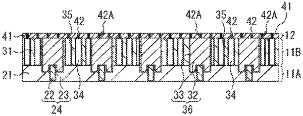
1. A semiconductor device, comprising:
a first layer including a first wiring and a first film;
a second layer including a second wiring and a second film; and
a third layer including a third film and a fourth film, wherein
the third layer is between the first layer and the second layer,
the first layer further includes:
an air gap between a first portion of the first film and a second portion of the first film, and
a fifth film between the first portion of the first film and the air gap, and
the fourth film is above or on the air gap,
the third film includes a plurality of holes, and
at least a part of the fourth film is in the plurality of holes.