| CPC H01L 21/76808 (2013.01) [H01L 21/76813 (2013.01); H01L 21/76816 (2013.01); H01L 21/31116 (2013.01); H01L 21/76834 (2013.01)] | 13 Claims |
|
1. A method for manufacturing a semiconductor device, comprising:
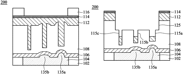
forming a metal layer in a substrate;
conformally forming a barrier layer on the substrate and covering the metal layer, wherein the barrier layer has an uneven top surface with a plurality of protrusions;
forming an insulating layer on the barrier layer;
performing a first etching step to form a plurality of openings in the insulating layer, wherein during the first etching step, a depth of the openings is controlled to avoid the openings exposing the barrier layer having the uneven top surface by controlling at least one etching parameter of the first etching step;
after the first etching step, forming a gap filling layer on the insulating layer and filling the opening, wherein the gap filling layer has a flat top surface;
forming a mask layer on the gap filling layer, and then forming a patterned photoresist layer on the mask layer to expose the mask layer located on the gap filling layer;
performing a second etching step on the mask layer, the gap filling layer and the insulating layer using the patterned photoresist layer as a mask to form a first via in the gap filling layer, and widening an upper portion of the openings to form a trench in the insulating layer communicating between the openings and the first via using the gap filling layer having the first via as a mask, wherein after the second etching step, a portion of the gap filling layer is located at a bottom of the openings;
performing a third etching step to remove the gap filling layer at the bottom of the openings and increasing a depth of the trench and the depth of the openings; and
forming a plurality of second vias communicating with the openings in the barrier layer having the uneven top surface to expose the metal layer, wherein the exposed surfaces of the metal layer are not leveled.
|