| CPC H01L 21/76224 (2013.01) [H01L 21/02271 (2013.01); H01L 21/0228 (2013.01); H01L 21/02282 (2013.01); H01L 29/0649 (2013.01)] | 18 Claims |
|
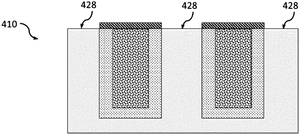
1. An integrated circuit structure, comprising:
a gap fill base layer comprising an electrically conductive material;
an opening extending into the gap fill base layer, the opening comprising a first sidewall and a second sidewall, the second sidewall laterally opposite the first sidewall, and the opening comprising a width and a depth, wherein an aspect ratio of the depth to the width is between 6 and 170;
a dielectric liner in the opening, the dielectric liner along the first sidewall of the opening and along the second sidewall of the opening with a remaining open volume between the dielectric liner along the first sidewall of the opening and along the second sidewall of the opening, the dielectric liner in lateral contact with the electrically conductive material of the gap fill base layer, and the dielectric liner having an uppermost surface;
a fill dielectric in the opening and on the dielectric liner, wherein the fill dielectric is a single material completely filling the remaining open volume between the dielectric liner along the first sidewall of the opening and along the second sidewall of the opening, the fill dielectric having an uppermost surface at a same level as the uppermost surface of the dielectric liner; and
a capping layer on the uppermost surface of the dielectric liner and on the uppermost surface of the fill dielectric, the capping layer having a dielectric material composition different than a dielectric composition of the fill dielectric.
|