| CPC H01L 21/67778 (2013.01) [H01L 21/324 (2013.01)] | 19 Claims |
|
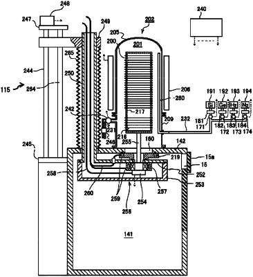
1. A method of manufacturing a semiconductor device, comprising:
(a) heating a substrate retainer in a reaction chamber, wherein the substrate retainer is provided with a plurality of slots capable of accommodating a plurality of substrates in a multistage manner;
(b) repeatedly performing a set comprising:
(b-1) moving the substrate retainer so as to locate one or more of the slots outside the reaction chamber; and
(b-2) charging one or more of the substrates into the one or more of the slots; and
(c) moving the substrate retainer such that the plurality of substrates charged in the plurality of slots are accommodated in the reaction chamber.
|