| CPC H01L 21/568 (2013.01) [H01L 21/561 (2013.01); H01L 21/78 (2013.01); H01L 23/3114 (2013.01); H01L 23/3121 (2013.01); H01L 23/3135 (2013.01); H01L 23/367 (2013.01); H01L 23/49838 (2013.01); H01L 23/528 (2013.01); H01L 24/19 (2013.01); H01L 24/96 (2013.01); H01L 25/0657 (2013.01); H01L 23/5389 (2013.01); H01L 2223/5448 (2013.01); H01L 2224/04105 (2013.01); H01L 2224/12105 (2013.01); H01L 2224/32225 (2013.01); H01L 2224/92144 (2013.01); H01L 2224/97 (2013.01); H01L 2924/19105 (2013.01)] | 20 Claims |
|
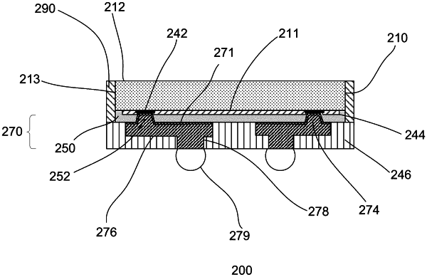
1. A semiconductor package comprising:
a die with active and inactive surfaces, wherein the active surface includes die pads on a back-end-of-line (BEOL) dielectric;
a buffer layer disposed on the active surface of the die, wherein the buffer layer includes a vibration damping composition to prevent cracking of the BEOL dielectric from a wafer singulation process;
via openings in the buffer layer to expose the die pads; and
via contacts disposed on the via openings to provide electrical connection to the die pads.
|