| CPC H01L 21/561 (2013.01) [H01L 21/3043 (2013.01); H01L 23/13 (2013.01); H01L 23/3135 (2013.01); H01L 25/0655 (2013.01); H01L 25/18 (2013.01); H01L 21/563 (2013.01); H01L 23/147 (2013.01); H01L 23/3185 (2013.01); H01L 23/3192 (2013.01); H01L 23/481 (2013.01); H01L 24/73 (2013.01); H01L 24/97 (2013.01); H01L 2224/73204 (2013.01)] | 20 Claims |
|
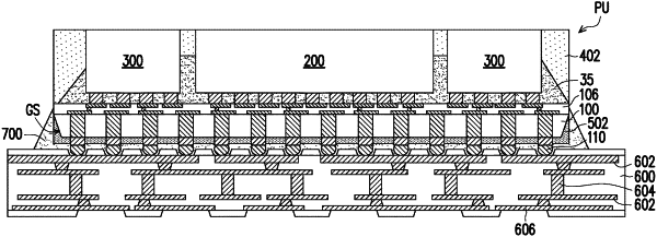
16. A semiconductor package, comprising:
an interposer having a first surface, a second surface opposite to the first surface and slant sidewalls extending from the second surface, wherein the interposer includes a substrate, conductive vias embedded within the substrate and a redistribution layer disposed on the substrate;
semiconductor dies, disposed on the first surface of the interposer and electrically connected with the interposer;
an encapsulant, disposed over the interposer and laterally encapsulating the semiconductor dies;
connectors, disposed on the second surface of the interposer and on the conductive vias; and
an insulative protection layer, disposed on the second surface of the interposer and surrounding the connectors, wherein the insulative protection layer has a peripheral drape portion physically contacts and covers the slant sidewalls of the interposer.
|