| CPC H01L 21/56 (2013.01) [H01L 21/78 (2013.01); H01L 23/291 (2013.01); H01L 23/293 (2013.01); H01L 23/3114 (2013.01)] | 20 Claims |
|
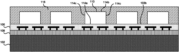
1. A method of manufacturing a semiconductor device, the method comprising:
electrically coupling a semiconductor die to a redistribution structure on a first carrier, the semiconductor die including a first surface facing the redistribution structure and a second surface spaced apart from the redistribution structure,
wherein the first carrier and the redistribution structure are coupled by a release layer between the first carrier and the redistribution structure;
reducing a thickness of the semiconductor die to no more than 10 μm;
coupling a flexible reinforcement structure to the second surface of the semiconductor die; and
separating the first carrier from the redistribution structure by dissolving the release layer or debonding the release layer from the redistribution structure.
|