| CPC H01L 21/4857 (2013.01) [C23C 18/1603 (2013.01); C23C 18/1803 (2013.01); C23C 18/38 (2013.01); C25D 3/38 (2013.01); C25D 5/02 (2013.01); C25D 5/34 (2013.01); C25D 7/00 (2013.01)] | 6 Claims |
|
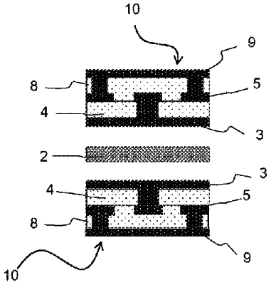
1. A method for manufacturing a package substrate for mounting a semiconductor device comprising an insulating layer and a wiring conductor provided on the insulating layer, the method comprising:
forming a first substrate comprising a first metal layer that has a thickness of 1 μm to 70 μm and that is peelable from a core resin layer, a first insulating resin layer, and a second metal layer in this order on one side or both sides of the core resin layer,
wherein the forming of the first substrate is performed by forming a first laminate in which the first metal layer, the first insulating resin layer, and the second metal layer are arranged in this order on both sides of the core resin layer, and heating and pressurizing the first laminate all at once to form the first substrate, and
wherein the core resin layer has a film thickness of 1 μm to 90 μm;
forming a non-through hole reaching a surface of the first metal layer on a surface of the first substrate, carrying out electrolytic copper plating and/or electroless copper plating on an inner wall of the non-through hole, and connecting the second metal layer and the first metal layer;
forming a second substrate by heating and pressurizing a second laminate formed by arranging a second insulating resin layer and a third metal layer in this order on a surface of the second metal layer of the first substrate;
forming a second non-through hole reaching the surface of the second metal layer on a surface of the second substrate, carrying out electrolytic copper plating and/or electroless copper plating on an inner wall of the second non-through hole, and connecting the second metal layer and the third metal layer;
peeling off, from the core resin layer, a third substrate comprising the first metal layer, the first insulating resin layer, the second metal layer, the second insulating resin layer, and the third metal layer in this order; and
patterning the first metal layer and the third metal layer of the third substrate to form the wiring conductor.
|