| CPC H01L 21/324 (2013.01) [H01J 37/321 (2013.01); H01J 37/32229 (2013.01); H01J 37/3244 (2013.01); H01J 37/32522 (2013.01); H01J 37/32724 (2013.01); H01L 21/31116 (2013.01); H01L 21/67069 (2013.01); H01L 21/67109 (2013.01)] | 17 Claims |

|
1. A method of manufacturing a semiconductor device, the method comprising:
loading a wafer into a wafer processing apparatus; and
processing the wafer in the wafer processing apparatus,
wherein the processing the wafer comprises
supplying a first process gas into the wafer processing apparatus using a shower head,
generating plasma using the first process gas,
supplying a second process gas using the shower head and mixing the second process gas with the plasma,
performing, at an first internal pressure of the wafer processing apparatus, a plasma process on the wafer using the plasma and the second process gas at a first temperature, and
performing, at a second internal pressure of the wafer processing apparatus less than the first internal pressure, an annealing process on the wafer at a second temperature higher than the first temperature after the performing the plasma process,
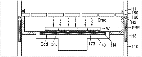
wherein the temperature of the wafer is determined by the difference between a heat gain of the wafer by a radiant heat from the showerhead and a heat loss of the wafer by heat convection by an internal atmosphere of the wafer processing apparatus, and
wherein the temperature of the wafer is decreased to the first temperature by increasing the internal pressure of the wafer processing apparatus to the first pressure to increase the heat loss by the heat convection between the wafer and the first and second process gases, and
the temperature of the wafer is increased to the second temperature by decreasing the internal pressure of the wafer processing apparatus to the second pressure to decrease the heat loss by the heat convection between the wafer and the first and second process gases.
|