| CPC H01L 21/324 (2013.01) [H01L 21/02057 (2013.01); H01L 21/02063 (2013.01); H01L 21/67115 (2013.01)] | 14 Claims |
|
1. A method of manufacturing a semiconductor device comprising:
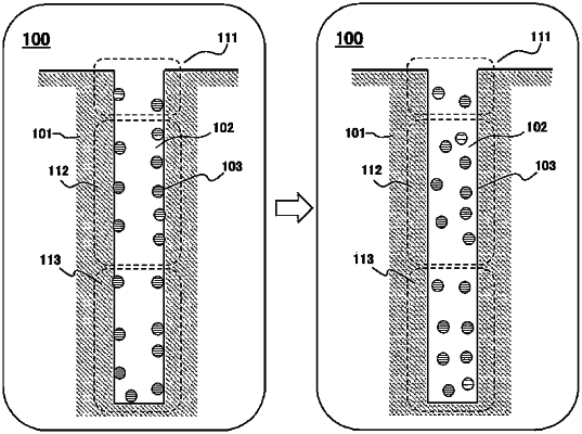
(a) loading a substrate on which a plurality of grooves are provided into a process chamber, wherein a residue is adhered to the plurality of the grooves;
(b) desorbing the residue from the plurality of the grooves by heating the substrate; and
(c) discharging the residue from the plurality of the grooves to a process space of the process chamber after (b) is performed by heating a surface of the substrate to a temperature higher than a temperature of the substrate in (b) such that a temperature of an upper region of the plurality of the grooves is higher than a temperature of a lower region of the plurality of the grooves,
wherein a first heater configured to heat the substrate through a back surface of the substrate and a second heater configured to heat the substrate through the surface of the substrate are provided in the process chamber, and
wherein the first heater is operated without operating the second heater in (b), and the second heater and the first heater are operated in (c).
|