| CPC H01L 21/32134 (2013.01) [H01L 29/66545 (2013.01)] | 7 Claims |
|
1. A method for a clean procedure during manufacturing a semiconductor device, comprising:
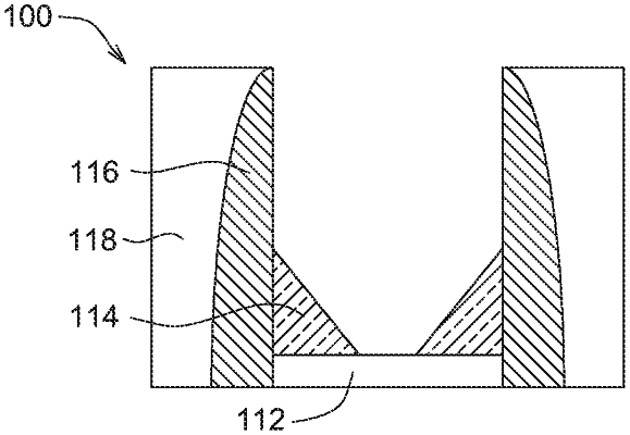
providing a patterned sacrificial gate structure comprising a gate dielectric and a sacrificial layer; wherein the patterned sacrificial gate structure is embedded in a dielectric layer and an upper surface of the sacrificial layer is exposed;
removing the sacrificial layer by performing a first etching process without etching the gate dielectric; and
removing a residue of the sacrificial layer by performing a hydrophilic treatment and a hydrophobic treatment,
wherein the hydrophilic treatment comprises a hydrophilic surface modification process, and the hydrophobic treatment comprises a hydrophobic surface modification process;
wherein the hydrophilic surface modification process comprises using an acidic oxidant, and the hydrophobic surface modification process comprises using a fluorinated acid;
wherein the hydrophilic treatment and the hydrophobic treatment are performed for at least 2 cycles.
|