| CPC H01L 21/3086 (2013.01) [H01L 21/0337 (2013.01)] | 15 Claims |
|
1. A patterning method, comprising:
providing a substrate, wherein the substrate comprises adjacent storage regions and peripheral circuit regions;
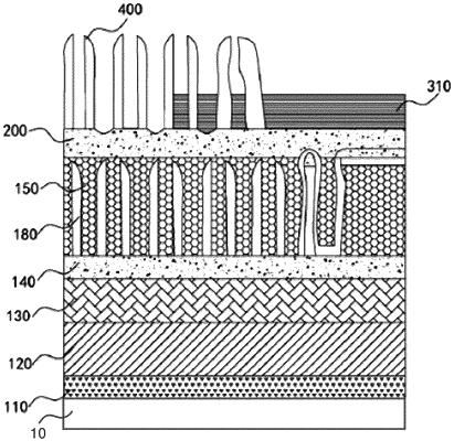
forming, on the substrate, a pattern transfer layer, the pattern transfer layer having a plurality of first hard masks, wherein the first hard masks extend along a first direction and are spaced apart from each other; and forming a barrier layer on the pattern transfer layer;
forming, on the barrier layer, a plurality of second hard masks, the plurality of second hard masks extending along a second direction, wherein the second hard masks are spaced apart from each other; and
the second hard masks are located in the storage regions and second hard masks close to the peripheral circuit regions have structural defects;
forming a first buffer layer on the barrier layer, and filling the second hard masks that have the structural defects with the first buffer layer, wherein an orthographic projection of the first buffer layer overlaps the peripheral circuit regions and a part of each of the storage regions; and
patterning the barrier layer and the pattern transfer layer by using the first buffer layer and second hard masks not filled with the first buffer layer as a mask.
|