| CPC H01L 21/3065 (2013.01) [H01L 21/0206 (2013.01); H01L 21/02178 (2013.01); H01L 21/0274 (2013.01); H01L 21/3081 (2013.01)] | 15 Claims |
|
1. A method for depositing, patterning, and removing a layer of aluminum oxide as a masking material layer for performing a reactive ion etching (RIE), the method comprising:
depositing a layer of first layer of photoresist onto a substrate surface of a substrate;
performing a lithography processing step on the first layer of photoresist by aligning a mask design to either pre-existing features made on the substrate surface or to attributes of the substrate, followed by exposure of the first layer of photoresist to transfer the desired shapes and dimensions of the features into the first layer of photoresist;
developing the first layer of photoresist thus patterning the first layer of photoresist into the desired shapes and dimensions of the mask design into the first layer of photoresist;
cleaning exposed regions of the substrate surface of any residual photoresist not removed during development;
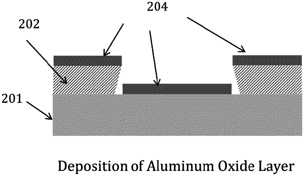
depositing a second thin-film layer of aluminum oxide onto the exposed regions of the substrate surface and the patterned first layer of photoresist wherein the second layer of thin-film layer of aluminum oxide has a thickness less than the thickness of the first layer of photoresist;
immersing the substrate into a solvent solution that dissolves the first layer of photoresist on the substrate thus causing the second layer of aluminum oxide positioned on top of the first layer of photoresist lift-off or be released from the substrate thereby leaving a patterned second layer of aluminum oxide layer on the substrate surface where no first layer of photoresist was present;
performing a reactive ion etching on the exposed positions of the substrate surface to a pre-determined depth into the substrate surface wherein the patterned second layer of aluminum oxide functions as a protective hard masking material layer on the substrate surface preventing etching from occurring where the patterned second layer of aluminum oxide is present; and
removing the second layer of aluminum oxide by immersion in a sodium hydroxide containing solution.
|