US 11,990,343 B2
Gate metal formation on gallium nitride or aluminum gallium nitride
Wayne Mack Struble, Franklin, MA (US); Timothy Edward Boles, Tyngsboro, MA (US); Jason Matthew Barrett, Amherst, NH (US); and John Stephen Atherton, Acton, MA (US)
Assigned to MACOM TECHNOLOGY SOLUTIONS HOLDINGS, INC., Lowell, MA (US)
Appl. No. 17/288,190
Filed by MACOM Technology Solutions Holdings, Inc., Lowell, MA (US)
PCT Filed Dec. 6, 2019, PCT No. PCT/US2019/064939
§ 371(c)(1), (2) Date Apr. 23, 2021,
PCT Pub. No. WO2020/118185, PCT Pub. Date Jun. 11, 2020.
Claims priority of provisional application 62/786,624, filed on Dec. 31, 2018.
Claims priority of provisional application 62/776,711, filed on Dec. 7, 2018.
Prior Publication US 2021/0407810 A1, Dec. 30, 2021
Int. Cl. H01L 21/285 (2006.01); H01L 21/033 (2006.01); H01L 29/20 (2006.01); H01L 29/40 (2006.01)
CPC H01L 21/28575 (2013.01) [H01L 21/0331 (2013.01); H01L 29/2003 (2013.01); H01L 29/401 (2013.01); H01L 29/402 (2013.01)] 20 Claims
OG exemplary drawing
 
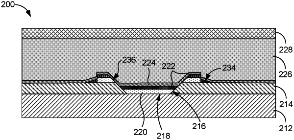
1. A method of manufacturing an electrode structure for a device, comprising:
forming an opening in a silicon nitride layer to expose a surface region of a substrate through the opening;
forming a photoresist layer over the silicon nitride layer and around the opening in the silicon nitride layer, the photoresist layer comprising a mask opening;
depositing a gate metal layer through the mask opening and onto the surface region of the substrate;
removing the photoresist layer; and
depositing a barrier metal layer over the gate metal layer and the silicon nitride layer.