| CPC H01L 21/28123 (2013.01) [H01L 21/02164 (2013.01); H01L 21/32135 (2013.01); H01L 21/76224 (2013.01); H01L 21/823431 (2013.01); H01L 21/823437 (2013.01); H01L 21/823468 (2013.01); H01L 21/823481 (2013.01); H01L 29/66545 (2013.01); H01L 29/66795 (2013.01)] | 20 Claims |

|
1. A method comprising:
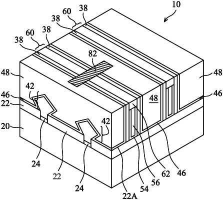
forming a gate stack extending over a semiconductor region;
forming gate spacers, wherein the gate spacers are on first sidewalls of the gate stack;
etching the gate stack to form a trench extending into the gate stack;
removing a dielectric layer from the trench to reveal second sidewalls of the gate stack, wherein the second sidewalls face the trench; and
filling the trench with a dielectric material to form a dielectric isolation region, wherein the dielectric isolation region contacts the second sidewalls of the gate stack.
|