| CPC H01L 21/0337 (2013.01) [H01L 21/0332 (2013.01); H01L 21/76802 (2013.01); H10B 12/01 (2023.02)] | 6 Claims |
|
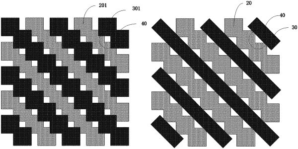
1. A method of manufacturing a semiconductor device, comprising:
providing a layer to be etched;
forming a patterned first mask layer on the layer to be etched, wherein the first mask layer comprises a plurality of first strip masks disposed parallel to each other
forming a patterned second mask layer on the layer to be etched, wherein the second mask layer comprises a plurality of second strip masks disposed parallel to each other, wherein the second mask layer and the first mask layer jointly defining openings to expose the layer to be etched and the plurality of first strip masks and the plurality of second strip masks are alternately disposed in parallel; and
etching the layer to be etched using the first mask layer and the second mask layer as masks thus forming a pattern to be etched;
wherein both sides of a first strip mask or both sides of a second strip mask comprise recesses that are arranged at regular intervals, wherein the recesses of the first strip mask jointly define the openings with the corresponding second strip mask, or the recesses of the second strip mask jointly define the openings with the corresponding first strip mask;
wherein the recesses are defined in a top view; wherein shape of the recesses comprises a triangle, an arc, or a rectangle.
|