| CPC H01L 21/0273 (2013.01) [G03F 7/094 (2013.01); G03F 7/20 (2013.01); G03F 7/32 (2013.01); H01L 21/0228 (2013.01); H01L 21/0332 (2013.01); H01L 21/0337 (2013.01); H01L 21/31111 (2013.01); G03F 7/095 (2013.01); H01L 21/30608 (2013.01)] | 20 Claims |
|
1. A method of manufacturing an integrated circuit device, the method comprising:
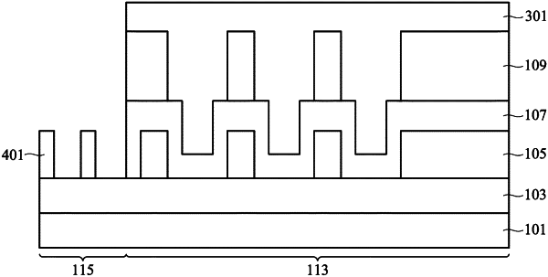
forming a first mandrel and a second mandrel over a substrate;
depositing a spacer material over both the first mandrel and the second mandrel and also between the first mandrel and the second mandrel;
depositing a bottom anti-reflective layer over the spacer material, a portion of the spacer material being exposed after the depositing the bottom anti-reflective layer;
applying an etchant to the spacer material through the bottom anti-reflective layer, the etchant etching the spacer material at a rate of no greater than about 4.2 Å/min; and
depositing a dielectric material in physical contact with a remaining portion of the spacer material.
|
|
8. A method of manufacturing an integrated circuit device, the method comprising:
depositing a spacer material over a substrate and between a first mandrel and a second mandrel;
depositing a photoresist over the spacer material;
forming an opening through the photoresist to expose the spacer material, the opening having a first aspect ratio;
etching the spacer material at a rate of no greater than about 4.2 Å/min, wherein after the etching the spacer material the opening has a second aspect ratio less than the first aspect ratio; and
depositing a dielectric material into the opening after the etching the spacer material.
|
|
15. A method of manufacturing a semiconductor device, the method comprising:
depositing a hard mask over a layer to be patterned;
forming a first mandrel and a second mandrel over the hard mask, the first mandrel being separated from the second mandrel by a first region;
partially filling the first region with a spacer material, wherein after the partially filling the first region a first opening extends into the first region;
placing an anti-reflective layer over the spacer material;
placing a middle layer over the anti-reflective layer;
patterning the anti-reflective layer to form a second opening over the first opening;
etching the middle layer to reduce a thickness of the middle layer; and
filling the first opening and at least part of the second opening with a dielectric material.
|