| CPC H01L 21/02532 (2013.01) [C30B 25/10 (2013.01); H01L 21/02433 (2013.01); H01L 21/0262 (2013.01); H01L 21/30625 (2013.01)] | 5 Claims |
|
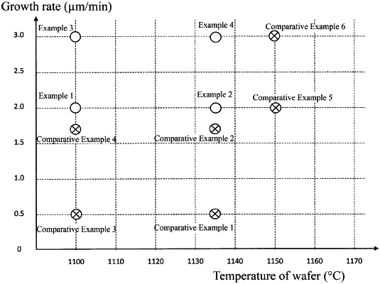
1. A method for producing a silicon epitaxial wafer in which an epitaxial layer is grown in a vapor phase on a principal plane of a silicon single crystal wafer, the principal plane being a plane or a plane having an off-angle of less than 1 degree from the plane, the method comprising:
setting a temperature of the silicon single crystal wafer to 1100° C. to 1135° C.; and
growing the epitaxial layer in the vapor phase at a growth rate of 2.0 μm/min to 3.0 μm/min so that a number of microscopic step defects having a height over 3 nm on a surface of the epitaxial layer when observed using a differential interference contrast method is 1.5/300 mm wafer or less.
|