| CPC H01L 21/02164 (2013.01) [H01L 21/02332 (2013.01); H01L 21/02334 (2013.01); H01L 21/324 (2013.01)] | 18 Claims |
|
1. A method for forming a silicon dioxide film, comprising:
providing a semiconductor substrate;
forming a silicon dioxide layer on the semiconductor substrate;
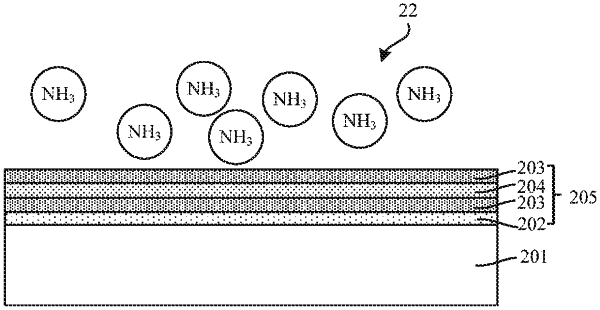
performing a nitrogen treatment to the silicon dioxide layer, such that a first portion of the silicon dioxide layer occupying a portion of a thickness of the silicon dioxide layer and disposed away from the semiconductor substrate is converted into a mixed layer of silicon nitride and silicon oxynitride, and a remaining portion of the silicon dioxide layer in contact with the semiconductor substrate is kept; and
removing the mixed layer such that the remaining portion of the silicon dioxide layer forms a silicon dioxide film on the semiconductor substrate.
|