| CPC H01J 37/32183 (2013.01) [B23K 15/0006 (2013.01); H01J 2237/327 (2013.01)] | 20 Claims |
|
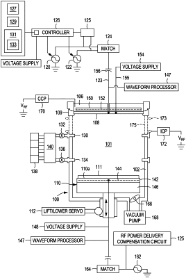
1. An RF power delivery compensation circuit, comprising:
a first input configured to receive an RF forward power from an RF power source connected to a processing chamber; and
a second input configured to receive an RF delivered power from a matching network connected between the RF power source and the processing chamber,
wherein the RF power delivery compensation circuit calculates an RF forward power compensation factor based on the RF forward power and the RF delivered power for adjusting the RF forward power delivered to the processing chamber during operation.
|