| CPC H01J 37/32183 (2013.01) [H01J 37/32724 (2013.01)] | 10 Claims |
|
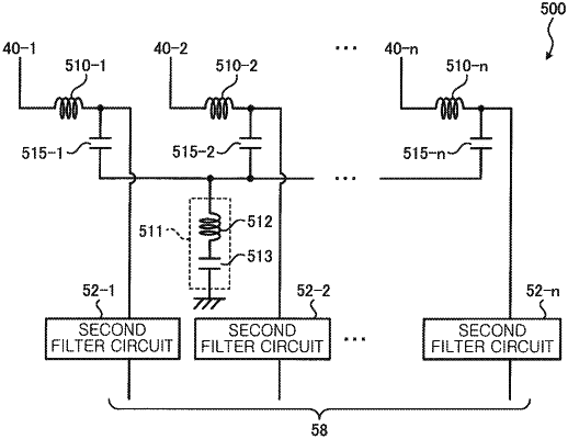
1. A filter circuit provided in a plasma processing device for processing a substrate using plasma generated using power of a first frequency of 4 MHz or more and power of a second frequency of 100 Hz or more and less than 4 MHz, the filter circuit comprising:
a first filter provided in a wiring between a conductive member provided in the plasma processing device and a power supply configured to supply power of a third frequency of less than 100 Hz or control power which is direct-current (DC) power, to the conductive member; and
a second filter provided in a wiring between the first filter and the power supply,
wherein the first filter includes:
a first coil which is connected to the wiring in series and which has no core material or has a first core material with a relative permeability of less than 10; and
a series resonant circuit which is connected between the wiring and a ground and which has a coil and a capacitor which are connected in series, and
wherein the second filter includes a second coil which is connected to the wiring provided between the first coil and the power supply in series and which has a second core material with a relative permeability of 10 or more.
|