| CPC H01G 4/30 (2013.01) [H01G 2/065 (2013.01); H01G 4/008 (2013.01); H01G 4/012 (2013.01); H01G 4/1218 (2013.01); H01G 4/224 (2013.01)] | 14 Claims |
|
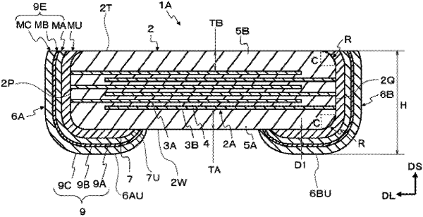
1. A ceramic electronic component comprising:
an element body including a dielectric and at least one internal electrode therein, the element body having a plurality of surfaces, the plurality of surfaces including a first surface and a second surface opposite the first surface; and
at least one external electrode formed on the element body, each of the at least one external electrode including a base layer and a plating layer formed on the base layer,
wherein the base layer is in contact with the internal electrode, contains a metal, and has a first end face adjacent to an outer periphery of the second surface of the element body, and the plating layer has a second end face adjacent to an outer periphery of the first end face such that the first and second end faces form, in combination, a multilayer structure on the outer periphery of the second surface of the element body,
wherein the element body has a curved chamfered surface at a ridge formed by the second surface, the base layer extends wrapping the curved chamfered surface up to a flat portion of the second surface, and the plating layer extends wrapping along a wrapping portion of the base layer that wraps the curved chamfered surface, and
wherein the first end face of the base layer is a horizontally flat surface that is level to the flat portion of second surface of the element body, and the second end face of the plating layer is a horizontally flat surface that is level to the plat portion of the second surface of the element body, thereby the first end face of the base layer and the second end face of the plating layer respectively being horizontally flat surfaces flush with each other exposed to an exterior and being coplanar with the plat portion of the second surface of the element body, and the external electrode not covering any portion of the second surface.
|