| CPC H01G 4/30 (2013.01) [H01G 4/008 (2013.01); H01G 4/012 (2013.01); H01G 4/1209 (2013.01)] | 19 Claims |
|
1. A multilayer ceramic capacitor comprising:
a laminate including a dielectric ceramic layer and an internal electrode layer that are laminated in a lamination direction; and
an external electrode connected to the internal electrode layer; wherein
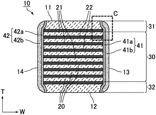
the laminate includes a first main surface and a second main surface that oppose each other in the lamination direction, a first lateral surface and a second lateral surface that oppose each other in a width direction perpendicular or substantially perpendicular to the lamination direction, and a first end surface and a second end surface that oppose each other in a length direction perpendicular or substantially perpendicular to the lamination direction and the width direction;
the internal electrode layer includes a first internal electrode layer extending to the first end surface and a second internal electrode layer extending to the second end surface so as to oppose the first internal electrode layer with the dielectric ceramic layer therebetween;
the external electrode includes a first external electrode disposed on the first end surface and connected to the first internal electrode layer, and a second external electrode disposed on the second end surface and connected to the second internal electrode layer;
the laminate includes a central layer portion in which the first internal electrode layer and the second internal electrode layer are alternately laminated with the dielectric ceramic layer therebetween, peripheral layer portions sandwiching the central layer portion in the lamination direction, and side margins sandwiching the central layer portion and the peripheral layer portions in the width direction;
each of the side margins includes an inner layer on an innermost side in the width direction and an outer layer on an outermost side in the width direction;
each of the inner layers is in contact with the central layer portion and the peripheral layer portions in the width direction;
a dimension of each of the inner layers in the lamination direction is greater than a dimension of the central layer portion in the lamination direction; and
when viewing the laminate through a cross section parallel or substantially parallel to the width direction and the lamination direction at a central portion in the length direction of the laminate, a point P indicates an end in the width direction of the internal electrode layer closest to the first main surface or the second main surface of the laminate, a point Q indicates a point where a boundary between the peripheral layer portions including the point P and the side margins including the point P intersects the first main surface or the second main surface of the laminate, and an imaginary line IL is drawn to pass through the point P and the point Q, the boundary is curved from the imaginary line IL.
|