| CPC H01G 11/06 (2013.01) [H01G 11/48 (2013.01); H01M 4/133 (2013.01); H01M 10/0525 (2013.01); H01M 10/0569 (2013.01)] | 5 Claims |
|
1. An electrochemical device comprising:
a positive electrode;
a negative electrode; and
an electrolytic solution, wherein:
the electrolytic solution contains an anion and a lithium ion,
the positive electrode includes a conductive polymer as a positive electrode active material that causes the electrochemical device to perform charging and discharging by doping and dedoping of the anion,
the negative electrode includes a negative electrode active material that causes the electrochemical device to perform charging and discharging by occluding and releasing the lithium ion,
the positive electrode includes an electrode current collector and an electrode material layer supported by the electrode current collector,
the electrode material layer includes at least the conductive polymer, and
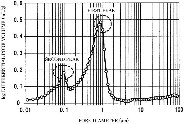
a log differential pore volume distribution of the electrode material layer has at least one peak in a range of a pore diameter of more than or equal to 50 nm.
|