| CPC H01F 27/28 (2013.01) [H01F 17/0013 (2013.01); H01F 27/29 (2013.01); H01F 27/292 (2013.01); H01F 27/323 (2013.01); H01F 41/04 (2013.01); H01F 41/041 (2013.01); H01F 41/10 (2013.01); H01F 41/122 (2013.01)] | 19 Claims |

|
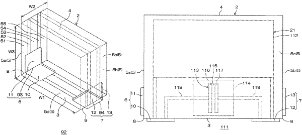
1. A chip component comprising:
a sealing body having mounting surface and a non-mounting surface that are formed in oblong shapes, the sealing body further having a first connecting surface and a second connecting surface connected to short sides of the mounting surface, and a third connecting surface and a fourth connecting surface connected to long sides of the mounting surface;
an inductor that is sealed inside the sealing body; and
a capacitor that is sealed inside the sealing body together with the inductor, wherein
the sealing body has a laminated structure in which a plurality of insulating layers are laminated from the third connecting surface to the fourth connecting surface,
the capacitor includes a first conductor and a second conductor that face each other across a dielectric portion in an orthogonal direction to a lamination direction of the plurality of insulating layers, and
the first conductor and the second conductor are formed in a plate shape extending along the lamination direction.
|