| CPC G11C 7/1039 (2013.01) [G11C 7/18 (2013.01)] | 6 Claims |
|
1. A memory device that uses a semiconductor element, in which a page is made up of a plurality of memory cells arranged in a row direction of a substrate, and a plurality of the pages is arranged in a column direction,
wherein each of the memory cells contained in each of the pages includes:
a semiconductor base material erected on the substrate in a vertical direction of the substrate or extended on the substrate in a horizontal direction,
a first impurity layer and a second impurity layer provided on opposite ends of the semiconductor base material,
a first gate insulating layer placed in contact with, or close to, the first impurity layer, partially or entirely surrounding a lateral surface of the semiconductor base material between the first impurity layer and the second impurity layer,
a second gate insulating layer joined to the first gate insulating layer and placed in contact with, or close to, the second impurity layer, surrounding the lateral surface of the semiconductor base material,
a first gate conductor layer covering part or all of the first gate insulating layer,
a second gate conductor layer covering the second gate insulating layer, and
a channel semiconductor layer in which the semiconductor base material is covered with the first gate insulating layer and the second gate insulating layer;
a positive hole group generated by an impact ionization phenomenon is held in the channel semiconductor layer by controlling voltages applied to the first gate conductor layer, the second gate conductor layer, the first impurity layer, and the second impurity layer;
during a page write operation, a voltage of the channel semiconductor layer is set to a first data retention voltage higher than a voltage/voltages of one or both of the first impurity layer and the second impurity layer;
during a page erase operation, by controlling voltages applied to the first impurity layer, the second impurity layer, the first gate conductor layer, and the second gate conductor layer, the positive hole group is pulled out from one or both of the first impurity layer and the second impurity layer, and the voltage of the channel semiconductor layer is set to a second data retention voltage lower than the first data retention voltage;
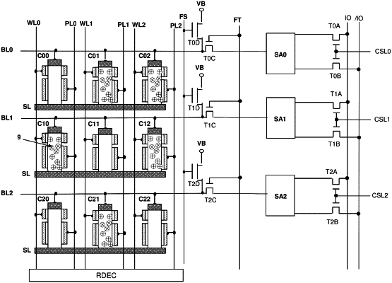
the first impurity layer of the memory cell is connected with a source line, the second impurity layer is connected with a bit line, one of the first gate conductor layer and the second gate conductor layer is connected with a word line, and another is connected with a drive control line;
the bit line is connected to a sense amplifier circuit via a switch circuit;
at least one of the word lines is selected and a refresh operation is performed to return the voltage of the channel semiconductor layer of the selected word line to the first data retention voltage by controlling voltages applied to the selected word line, the drive control line, the source line, and the bit line and thereby forming the positive hole group by an impact ionization phenomenon in the channel semiconductor layer of the memory cell in which the voltage of the channel semiconductor layer is set to the first data retention voltage using the page write operation; and
concurrently with the refresh operation, a page read operation is performed to read page data of a first memory cell group belonging to a first page into the sense amplifier circuit by placing the switch circuit in a nonconducting state.
|