| CPC G11C 29/4401 (2013.01) [G11C 29/12005 (2013.01); G11C 29/18 (2013.01); H03K 19/21 (2013.01); G11C 2029/1802 (2013.01)] | 20 Claims |

|
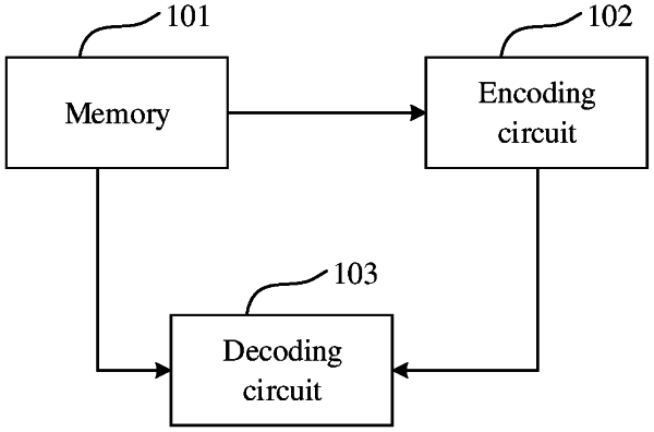
1. A storage system, comprising:
a memory, configured to write or read a plurality of data bits during a read-write operation, the plurality of data bits being divided into M bytes, and each byte having N data bits; and
an encoding circuit, configured to:
generate X first check codes based on two or more data bits of the plurality of data bits in each byte in an encoding stage, bit locations of the two or more data bits corresponding to a same first check code being identical in different bytes;
generate Y second check codes based on all data of two or more bytes of the M bytes in the encoding stage; and
generate a third check code based on the plurality of data bits, the X first check codes and the Y second check codes;
wherein the X first check codes, the Y second check codes and the third check code are used to determine an error state of the plurality of data bits; and
wherein when the plurality of data bits have a 1-bit error, the Y second check codes are used to locate a specific byte having the 1-bit error, and
the X first check codes are used to locate a specific bit having the 1-bit error; and
wherein M, N, X, and Y are all positive natural numbers.
|