| CPC G11C 19/28 (2013.01) [H03K 3/037 (2013.01); H03K 19/20 (2013.01)] | 20 Claims |
|
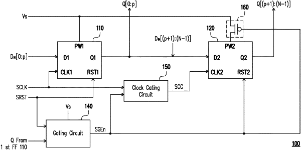
1. A shift register, comprising:
a first flip-flop (FF), including an input terminal coupled to a first portion of input data, an output terminal, and a clock terminal coupled to a clock signal;
a second FF, including an input terminal coupled to a second portion of input data, an output terminal, a clock terminal, a power terminal coupled to a supply power, wherein the second portion of the input data is subsequent to the first portion of the input data; and
a gating circuit, coupled between the output terminal of the first FF and the clock terminal of the second FF, and configured to disable the second FF for storing the second portion of a subsequent input data according to output data currently being stored in the first FF during at least one writing cycle where the entire input data is being written to the shift register.
|