| CPC G11C 17/18 (2013.01) [G11C 7/1069 (2013.01); G11C 7/20 (2013.01)] | 4 Claims |
|
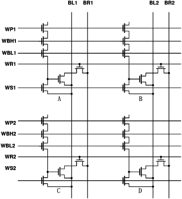
1. A one time programmable (OTP) memory array, comprising M×N OTP memories, wherein the OTP memories each comprise a storage metal oxide semiconductor (MOS) transistor (C0), a first MOS transistor (M1), a second MOS transistor (M2) and a detection MOS transistor (M0), a current connection terminal of the first MOS transistor (M1) is connected to a first current connection terminal of the detection MOS transistor (M0), a control terminal of the detection MOS transistor (M0) is connected to a current connection point of the second MOS transistor (M2), the control terminal of the detection MOS transistor (M0) is further connected to the storage MOS transistor (C0), an isolation module is disposed between the control terminal of the detection MOS transistor (M0) and the storage MOS transistor (C0), the storage MOS transistor is a Native MOS transistor, and M and N are both integers greater than 1;
wherein,
the isolation module comprises at least one isolation MOS transistor, and the isolation MOS transistor is a Native MOS transistor; and
in the array, a gate of each storage MOS transistor is connected to a same storage control point, each isolation MOS transistor is distinguished based on a distance from the storage MOS transistor, and gates of isolation MOS transistors with a same distance from the storage MOS transistor are connected to a same isolation control point.
|