| CPC G11C 16/3427 (2013.01) [G11C 16/0483 (2013.01); G11C 16/08 (2013.01); G11C 16/10 (2013.01); G11C 16/16 (2013.01); G11C 16/26 (2013.01); G11C 16/32 (2013.01); G11C 16/3418 (2013.01); G11C 16/3459 (2013.01)] | 11 Claims |
|
1. A memory device comprising:
a semiconductor substrate having a main surface extending in a first direction and a second direction crossing the first direction;
a bit line provided on a side of the main surface in a third direction that crosses the first direction and the second direction and extending the first direction;
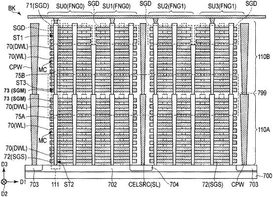
a first semiconductor pillar electrically connected to the bit line and extending in the third direction, the first semiconductor pillar having a first joint portion at a position in the third direction;
a second semiconductor pillar electrically connected to the bit line and extending in the third direction, the second semiconductor pillar having a second joint portion at the same position with the first joint portion in the third direction;
a first conductive member extending in the second direction and intersecting the first semiconductor pillar, the first conductive member being provided between the first joint portion and the bit line;
a second conductive member extending in the second direction and intersecting the second semiconductor pillar, the first and second conductive members being at a same position in the third direction, the second conductive member being electrically disconnected from the first conductive member;
a third conductive member extending in the second direction and intersecting the first semiconductor pillar, the third conductive member being provided between the first joint portion and the semiconductor substrate in the third direction;
a fourth conductive member extending in the second direction and intersecting the second semiconductor pillar, the third and fourth conductive members being at a same position in the third direction, the fourth conductive member being electrically disconnected from the third conductive member;
a fifth conductive member extending in the second direction and intersecting the first semiconductor pillar, the fifth conductive member being provided between the first conductive member and the bit line;
a sixth conductive member extending in the second direction and intersecting the second semiconductor pillar, the fifth and sixth conductive members being at a same position in the third direction, the sixth conductive member being electrically connected to the fifth conductive member;
a seventh conductive member extending in the second direction and intersecting the first semiconductor pillar, the seventh conductive member being provided between the substrate and the first joint portion; and
an eighth conductive member extending in the second direction and intersecting the second semiconductor pillar, the seventh and eighth conductive members being at a same position in the third direction, the eighth conductive member being electrically connected to the seventh conductive member.
|