| CPC G11C 13/0069 (2013.01) [G11C 11/1655 (2013.01); G11C 11/1675 (2013.01); G11C 13/0026 (2013.01); G11C 13/0004 (2013.01)] | 20 Claims |

|
1. A method, comprising:
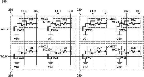
programming a first bit of a physical unclonable function into a first memory cell;
programming a second bit of the physical unclonable function into a second memory cell different from the first memory cell; and
generating, by a first memory circuit in the first memory cell, a first current indicating a logic value of the first bit,
wherein programming the first bit comprises:
turning on a first switch in the first memory circuit and at least one second switch in at least one second memory circuit in the first memory cell in response to a first bit line signal, to program one of the first memory circuit and the at least one second memory circuit while rest of the first memory circuit and the at least one second memory circuit is not programmed, according to the first bit line signal, and
wherein programming the second bit comprises:
receiving the first bit line signal by a first memory element in the second memory cell; and
programming the first memory element by turning on a third switch coupled to the first memory element,
wherein a control terminal of the third switch and a control terminal of the first switch are configured to receive the same control signal.
|