| CPC G11C 11/4099 (2013.01) [G06N 3/063 (2013.01); G11C 5/06 (2013.01); G11C 7/16 (2013.01); G11C 11/4074 (2013.01); G11C 11/4076 (2013.01); G11C 11/4085 (2013.01); G11C 11/4094 (2013.01); G11C 11/54 (2013.01)] | 3 Claims |
|
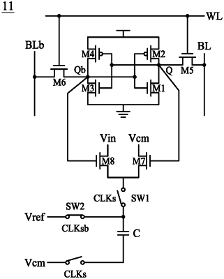
1. A static random-access memory (SRAM) cell, comprising:
a first inverter connected between ground and a power;
a second inverter connected between the ground and the power, the first inverter and the second inverter being cross-coupled;
a first access transistor that accesses an output of the first inverter under control of a word line, the output of the first inverter being then transferred via a first bit line;
a second access transistor that accesses an output of the second inverter under control of the word line, the output of the second inverter being then transferred via a second bit line;
a first passage transistor that passes a common-mode voltage, controlled by the output of the first inverter;
a second passage transistor that passes an input signal, controlled by the output of the second inverter;
a capacitor switchably coupled to receive the common-mode voltage and the input signal through the first passage transistor and the second passage transistor respectively; and
a switch, via which the capacitor is switchably connected to outputs of the first passage transistor and the second passage transistor, the switch being controlled by a sample clock signal.
|