| CPC G11C 11/4093 (2013.01) [G11C 5/02 (2013.01); G11C 5/025 (2013.01); G11C 5/04 (2013.01); G11C 11/406 (2013.01); G11C 11/4096 (2013.01); H01L 23/481 (2013.01); H01L 25/0652 (2013.01); H01L 25/0657 (2013.01); H01L 25/105 (2013.01); H01L 25/18 (2013.01); H01L 24/73 (2013.01); H01L 2224/0401 (2013.01); H01L 2224/16225 (2013.01); H01L 2224/32145 (2013.01); H01L 2224/32225 (2013.01); H01L 2224/48091 (2013.01); H01L 2224/48225 (2013.01); H01L 2224/48227 (2013.01); H01L 2224/73265 (2013.01); H01L 2225/0651 (2013.01); H01L 2225/0652 (2013.01); H01L 2225/06541 (2013.01); H01L 2225/06558 (2013.01); H01L 2225/06562 (2013.01); H01L 2225/1023 (2013.01); H01L 2225/1058 (2013.01); H01L 2924/00011 (2013.01); H01L 2924/00014 (2013.01); H01L 2924/01019 (2013.01); H01L 2924/01055 (2013.01); H01L 2924/14 (2013.01); H01L 2924/15311 (2013.01); H01L 2924/15321 (2013.01); H01L 2924/15331 (2013.01); H01L 2924/3011 (2013.01)] | 20 Claims |

|
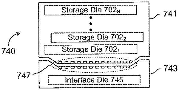
1. A memory device, comprising:
a logic integrated circuit (IC) base die, the logic IC base die including a primary interface for communicating with memory control circuitry, and multiple independent secondary interfaces; and
multiple memory die stacked on the logic IC base die, each of the multiple memory die including at least one independent memory interface coupled to a corresponding one of the multiple independent secondary interfaces of the logic IC base die in a dedicated manner using through-silicon-via (TSV) paths.
|