| CPC G11C 11/1659 (2013.01) [G11C 11/161 (2013.01); H10B 61/00 (2023.02); H10N 50/01 (2023.02); H10N 50/80 (2023.02); G11C 11/1655 (2013.01); G11C 11/1657 (2013.01); H10N 50/85 (2023.02)] | 20 Claims |
|
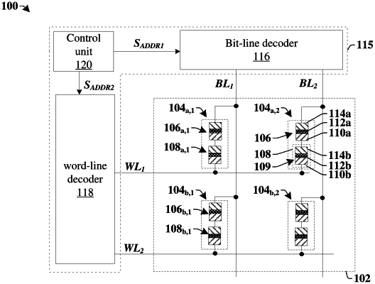
1. An integrated chip, comprising:
an operative memory device coupled to a bit-line, wherein the operative memory device is configured to store a data state;
a regulating access apparatus coupled between the operative memory device and a first word-line, wherein the regulating access apparatus comprises one or more regulating MTJ devices that are configured to control a current provided to the operative memory device; and
wherein the one or more regulating MTJ devices respectively comprise a free layer, a dielectric barrier layer on the free layer, and a pinned layer separated from the free layer by the dielectric barrier layer, wherein the pinned layer covers a center of an entire upper surface of the dielectric barrier layer, the entire upper surface of the dielectric barrier layer facing towards the pinned layer and extending between opposing outermost sidewalls of the dielectric barrier layer.
|