| CPC G11C 11/165 (2013.01) [G11C 11/161 (2013.01)] | 20 Claims |

|
1. A magnetic device, comprising:
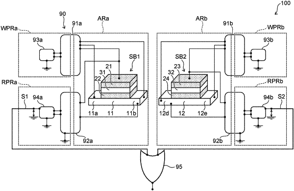
a first conductive portion including a first region, a second region, a third region between the first region and the second region, a direction from the first region to the second region being along a first direction;
a first stacked body including a first magnetic layer and a second magnetic layer, the second magnetic layer being between the third region and the first magnetic layer in a second direction crossing the first direction;
a second conductive portion including a fourth region, a fifth region, and a sixth region between the fourth region and the fifth region, a direction from the fourth region to the fifth region being along a third direction;
a second stacked body including a third magnetic layer and a fourth magnetic layer, the fourth magnetic layer being between the sixth region and the third magnetic layer in a fourth direction crossing the third direction; and
a controller,
the first stacked body being configured to be either in a first low electrical resistance state or in a first high electrical resistance state, the first high electrical resistance state having an electrical resistance higher than an electrical resistance of the first low electrical resistance state,
the second stacked body being configured to be either in a second low electrical resistance state or in a second high electrical resistance state, the second high electrical resistance state having an electrical resistance higher than an electrical resistance of the second low electrical resistance state,
the controller being configured to implement an initialization operation, a first operation, and a second operation, and implement an XNOR operation of a first input and a second input,
the controller being configured to set the first stacked body in a first resistance state of the first low electrical resistance state or the first high electrical resistance state, and set the second stacked body in a second resistance state of the second low electrical resistance state or the second high electrical resistance state in the first initialization operation,
the controller being configured to supply a first current to the first conductive portion while setting a potential of the first magnetic layer to a first set potential, and supply a second current to the second conductive portion while setting a potential of the third magnetic layer to a second set potential in the first operation,
an orientation of the first current in the first operation when the first input is “0” being opposite to an orientation of the first current in the first operation when the first input is “1”,
an orientation of the second current in the first operation when the first input is “0” being opposite to an orientation of the second current in the first operation when the first input is “1”,
a first polarity of the first set potential in the first operation when the second input is “1”, with reference to the first set potential in the first operation when the second input is “0” being opposite to a second polarity of the second set potential in the first operation when the second input is “1”, with reference to the second set potential in the first operation when the second input is “0”, and
the controller being configured to measure values corresponding to an electrical resistance of the first stacked body after the first operation and an electrical resistance of the second stacked body after the first operation in the second operation.
|