US 11,990,166 B2
Ferroelectric recording medium and ferroelectric storage apparatus
Masaaki Yanagisawa, Tokyo (JP)
Assigned to RESONAC CORPORATION, Tokyo (JP)
Filed by Resonac Corporation, Tokyo (JP)
Filed on May 12, 2023, as Appl. No. 18/316,641.
Application 18/316,641 is a division of application No. 17/557,537, filed on Dec. 21, 2021, granted, now 11,705,157.
Claims priority of application No. 2020-219654 (JP), filed on Dec. 28, 2020; application No. 2020-219655 (JP), filed on Dec. 28, 2020; application No. 2020-219656 (JP), filed on Dec. 28, 2020; application No. 2020-219657 (JP), filed on Dec. 28, 2020; application No. 2020-219658 (JP), filed on Dec. 28, 2020; application No. 2020-219659 (JP), filed on Dec. 28, 2020; application No. 2020-219660 (JP), filed on Dec. 28, 2020; application No. 2020-219661 (JP), filed on Dec. 28, 2020; application No. 2020-219662 (JP), filed on Dec. 28, 2020; application No. 2020-219663 (JP), filed on Dec. 28, 2020; application No. 2020-219664 (JP), filed on Dec. 28, 2020; application No. 2020-219665 (JP), filed on Dec. 28, 2020; application No. 2021-050640 (JP), filed on Mar. 24, 2021; application No. 2021-050641 (JP), filed on Mar. 24, 2021; application No. 2021-068376 (JP), filed on Apr. 14, 2021; application No. 2021-098592 (JP), filed on Jun. 14, 2021; application No. 2021-101046 (JP), filed on Jun. 17, 2021; application No. 2021-117508 (JP), filed on Jul. 16, 2021; and application No. 2021-160168 (JP), filed on Sep. 29, 2021.
Prior Publication US 2023/0282235 A1, Sep. 7, 2023
This patent is subject to a terminal disclaimer.
Int. Cl. G11B 9/02 (2006.01); G11C 11/22 (2006.01); G11C 11/56 (2006.01); G11B 5/21 (2006.01)
CPC G11B 9/02 (2013.01) [G11C 11/22 (2013.01); G11C 11/221 (2013.01); G11C 11/5657 (2013.01); G11B 5/21 (2013.01)] 9 Claims
OG exemplary drawing
 
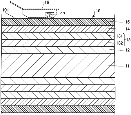
1. A ferroelectric recording medium including an electrode layer, a ferroelectric recording layer, and a protection layer formed in this order on a substrate,
wherein the ferroelectric recording layer includes a ferroelectric layer,
a lattice constant of a material constituting the ferroelectric layer and a lattice constant of a material constituting the electrode layer or the substrate are lattice-matched within a range of ±10%,
the ferroelectric layer has an amorphous structure with short-range order,
a distance of the short-range order is equal to or less than 2 nm, and
a lattice constant of the amorphous structure and the lattice constant of the material constituting the substrate are lattice-matched within a range of ±10%.