| CPC G09G 5/04 (2013.01) [G09G 2300/0452 (2013.01); G09G 2330/08 (2013.01); G09G 2330/10 (2013.01)] | 8 Claims |
|
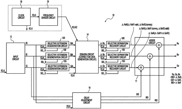
1. An input signal correction device for correcting input signals for a display panel in which numbers of R, G and B subpixels are equal or unequal at a ratio of minority subpixels to majority subpixels of 1:N, where N is an integer of 2 or more, comprising:
an input circuit configured to operate at operating frequency f, and for each of the R, G and B subpixels, to receive input of an input signal;
an extension/degeneration circuit configured to operate at operating frequency f and to receive input of a first control signal and, for each of the R, G and B subpixels, output a preprocessing signal by increasing a cycle length of the input signal by a factor of N or output a preprocessing signal by degenerating the input signal to 1/N, based on the first control signal;
a correction circuit configured to operate at operating frequency f/N and, for each of the R, G and B subpixels, to output a correction signal by correcting the preprocessing signal;
a separation/recovery circuit configured to operate at operating frequency f and to receive input of a second control signal and, for each of the R, G and B subpixels, output a differential signal by reducing the cycle length of the correction signal to 1/N or reduce the cycle length of the correction signal to 1/N and output a same differential signal over N cycles, based on the second control signal;
a delay adjustment circuit configured to operate at operating frequency f, and for each of the R, G and B subpixels, to output a delay signal by delaying the input signal; and
an adder circuit configured to, for each of the R, G and B subpixels, add the differential signal to the delay signal.
|