| CPC G09G 3/3685 (2013.01) [G09G 3/006 (2013.01); G09G 3/2096 (2013.01); G09G 3/3688 (2013.01); G09G 3/3696 (2013.01); G09G 2310/08 (2013.01); G09G 2330/12 (2013.01); G09G 2370/08 (2013.01); G09G 2370/14 (2013.01)] | 2 Claims |
|
1. A source driver that drives a display device based on a plurality of data signals, comprising:
an interface circuit that receives a clock signal and the plurality of data signals and that outputs the plurality of data signals in accordance with a clock timing of the clock signal;
a latch circuit that receives the plurality of data signals outputted from the interface circuit and that outputs the plurality of data signals in a successive order corresponding to pixel columns of the display device in a scanning line direction;
a gradation voltage conversion circuit that converts the plurality of data signals outputted from the latch circuit to gradation voltages corresponding to luminance gradations represented by the plurality of data signals outputted from the latch circuit; and
an output circuit that separately amplifies each of the gradation voltages and outputs the amplified gradation voltages as driving signals of the display device,
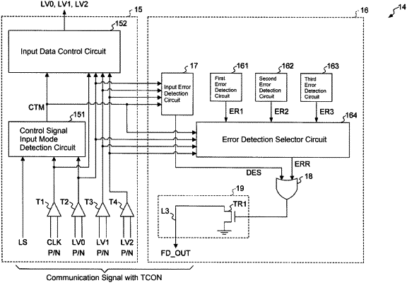
wherein the interface circuit comprises:
a timing signal generating circuit that receives the clock signal and that generates a timing signal indicating a timing to switch between a data input period in which the plurality of data signals are supplied to a data latch circuit and a non-input period in which the supply of the plurality of data signals is stopped, based on at least one of the plurality of data signals and the clock signal;
a data control circuit that controls the supply of the plurality of data signals to the data latch circuit based on the timing signal;
a plurality of driver error detection circuits that detect an error in the source driver;
a selector circuit that selects one of the plurality of driver error detection circuits based on the plurality of data signals during the non-input period, and outputs a driver error detection signal indicating a detection result of the selected driver error detection circuit at a timing corresponding to the timing signal and the clock signal;
an input error detection circuit that detects an error in data input of the plurality of data signals and outputs an input error detection signal indicating a detection result;
an OR circuit that outputs an OR signal indicating a logical disjunction of the driver error detection signal and the input error detection signal; and
a signal output unit that includes a first conductivity-type MOS transistor having a gate terminal connected to an output part of the OR circuit and a source terminal connected to a prescribed potential, and a signal output line connected to a drain terminal of the MOS transistor.
|