| CPC G09G 3/3266 (2013.01) [G09G 3/3275 (2013.01); G09G 3/3614 (2013.01); G09G 3/3677 (2013.01); G09G 3/3688 (2013.01); G09G 2310/0254 (2013.01); G09G 2310/08 (2013.01); G09G 2330/04 (2013.01)] | 18 Claims |
|
11. A display device, comprising a display panel and a display driving structure, wherein the display driving structure is configured to drive the display panel, wherein at least one pixel group comprises N rows and M columns of sub-pixels, N scan lines and M data lines, an m-th column of the sub-pixels in the at least one pixel group is all connected to an m-th data line, and at least part of the sub-pixels in an n-th row in the at least one pixel group are connected to an n-th scan line, where 1≤m≤N, 1≤m≤M, and N≥3;
wherein the display driving structure comprises:
a drive component connected to data lines in the at least one pixel group, wherein the drive component provides a one-to-one corresponding data signal to each of the sub-pixels through the data lines; and
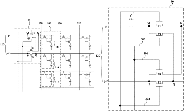
at least one switching component that is in one-to-one correspondence with the at least one pixel group, wherein the at least one switching component has a control terminal, a first input terminal, a second input terminal, a first output terminal and a second output terminal, wherein the first input terminal is configured to receive a p-th row of scanning signals, the second input terminal is configured to receive a (p+1)-th row of scanning signals, wherein the (p+1)-th row of the scanning signals is output after the p-th row of the scanning signals; wherein the first output terminal is connected to a p-th row of scan lines in the at least one pixel group, and the second output terminal is connected to a (p+1)-th row of scan lines in the at least one pixel group, where 1≤p<N;
wherein the control terminal of the at least one switching component is configured to control conduction of the first input terminal and the second output terminal, and control conduction of the second input terminal and the first output terminal when data signals received by adjacent two sub-pixels connected to each column of the data lines are different in polarity, wherein a write time of a data signal of a sub-pixel connected to the (p+1)-th row of the scan lines is prior to that of a data signal of a sub-pixel connected to the p-th row of the scan lines; and
wherein the control terminal of the at least one switching component is further configured to control conduction of the first input terminal and the first output terminal, and control conduction of the second input terminal and the second output terminal when data signals received by adjacent two sub-pixels connected to each column of the data lines are same in polarity, wherein a write time of the data signal of the sub-pixel connected to the p-th row of the scan lines is prior to that of the data signal of the sub-pixel connected to the (p+1)-th row of the scan lines.
|