| CPC G09G 3/3266 (2013.01) [G09G 3/3275 (2013.01); G11C 19/287 (2013.01); G09G 2310/0278 (2013.01); G09G 2310/0286 (2013.01); G09G 2310/061 (2013.01); G09G 2320/0247 (2013.01)] | 20 Claims |
|
1. A display drive circuit of a display panel, wherein the display panel includes display units arranged in an array; a display unit includes a light-emitting element and a pixel circuit connected to the light-emitting element; and the pixel circuit includes:
a drive transistor, wherein a gate electrode of the drive transistor is connected to a first node, a first electrode of the drive transistor is connected to a second node, and a second electrode of the drive transistor is connected to a third node;
a first reset transistor, wherein a gate electrode of the first reset transistor is configured to input a first signal, a first electrode of the first reset transistor is configured to input a reference voltage, and a second electrode of the first reset transistor is connected to the first node;
a compensation transistor, wherein a gate electrode of the compensation transistor is configured to input a second signal, a first electrode of the compensation transistor is connected to the first node, and a second electrode of the compensation transistor is connected to the third node; and
a data write transistor, wherein a gate electrode of the data write transistor is configured to input a third signal, and a first electrode of the data write transistor is configured to input a data signal, wherein the first signal and the second signal have a same period; and the display drive circuit comprising:
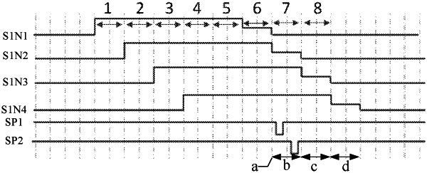
first shift registers from a first shift register of a 1st-stage to a first shift register of an Nth-stage, wherein N is a positive integer greater than 1, wherein first shift registers of first A stages are virtual shift registers which are at least configured to make that the inputted second signal of a same pixel circuit has a delay of a set time length t relative to the first signal; A is a positive integer greater than 1; and first shift registers of last (N-A) stages are at least configured to provide pixel circuits with the second signal;
wherein:
t=a+b+c+d; A=t/t0*X; a is a delay of a turn-on time segment of the third signal relative to a first time; the first time is a time when the first signal is turned off; d is a switching time length of the second signal; X is a row number of display units connected to a first shift register of each stage in the first shift registers of the last (N-A) stages; t0 is a normalization coefficient of b; and t0,>0; wherein: when X=1, the first shift register of each stage in the first shift registers of the last (N-A) stages is connected to one row of display units; b is a data write time length of the one row of display units; and c is a constant 0; or when X>1, the first shift register of each stage in the first shift registers of the last (N-A) stages is correspondingly connected to X rows of display units which are consecutively arranged; b is a data write time length of the X rows of display units which are arranged consecutively and connected to a first shift register of a same stage; c is a delay of a third time relative to a second time; the second time is a data write end time of the X rows of display units which are arranged consecutively and connected to the first shift register of the same stage; and the third time is a switch switching time of the second signal.
|