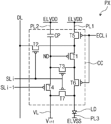
| CPC G09G 3/3266 (2013.01) [G06F 1/1652 (2013.01); G09F 9/301 (2013.01); G09G 3/3291 (2013.01); G09G 2380/02 (2013.01)] | 19 Claims |

|
1. A display module, comprising:
a base including a plurality of unit portions, each of the plurality of unit portions including a first portion and a plurality of second portions extending from the first portion and connecting adjacent first portions;
a gate pattern overlapped with the first portion, the gate pattern not extending over the plurality of second portions;
a first insulating layer disposed on the base to cover the gate pattern, the first insulating layer being overlapped with the first portion and the plurality of second portions and comprising a first contact hole defined therein;
a plurality of first lines which are disposed on the first insulating layer, each of the plurality of first lines being overlapped with at least one of the plurality of second portions, and at least one of the plurality of first lines being electrically connected to the gate pattern through the first contact hole;
a second insulating layer disposed on the plurality of first lines;
a plurality of second lines which are disposed on the second insulating layer, each of the plurality of second lines being overlapped with at least one of the plurality of second portions;
a third insulating layer disposed on the plurality of second lines; and
a plurality of third lines which are disposed on the third insulating layer, each of the plurality of third lines being overlapped with at least one of the plurality of second portions,
wherein the gate pattern comprises a first conductive material and each of the plurality of first lines, the plurality of second lines, and the plurality of third lines comprises a conductive material different from the first conductive material.
|